Introduction
In this article, we are going to learn about the GPU architecture and why and how it differs from the CPU architecture. A CPU is designed to execute a smaller number of instructions as quickly as possible whereas a GPU is designed to execute thousands of simple operations on a massive amount of data simultaneously.
The CPU has one simple goal, and that is to minimize latency. Because the next instruction could be anything so due to this uncertainty the CPU is designed in such a way that it executes one thread as fast as possible.
This is called latency optimization.
Whereas in the case of a GPU, it is designed to maximize the throughput (the number of instructions processed in a unit time).
GPUs were originally created for gaming because in 3D graphics, it is required to calculate millions of pixel simultaneously in order to render it on the screen in near real time which resulted in higher frame rates, massive pixel count and real time physics etc.
So instead of executing on complex program like the CPU, it receives millions of independent tasks.
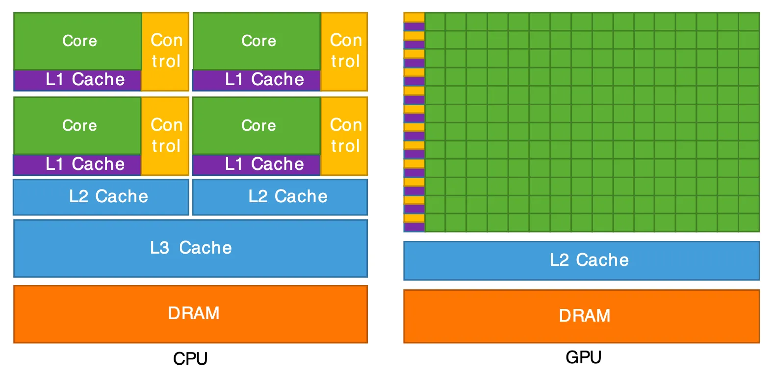
On the left is the CPU, it consists of lower number of cores and a larger control block and L1 Cache and beneath the cores are L2 Cache and L3 Cache. This shows that CPU spends most of its portion of transistors on control logic and cache memory which leaves fewer cores on the chip.
Large number of cache exists in the CPU because it has to keep lots of data as close to the CPU cores as fetching data from the DRAM is slower.
And on the right is the GPU diagram, as you can see that it has a very significant number of cores while the size of the control block and L1 Cache is very small, this indicates that the majority of the silicon is dedicated for the cores and a large L2 Cache.
Compared to a CPU, the GPU dedicates much less area to caching because its strategy for hiding memory latency is different. Rather than relying heavily on caches, it keeps thousands of threads ready to execute. If one group of threads waits for data from DRAM, another group immediately takes its place.
Architectural View of GPU
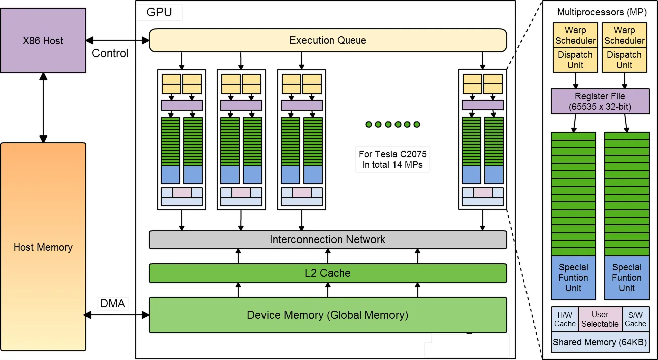
In this section I will explain the high level GPU architecture.
At a high level, the GPU architecture can be divided into four major subsystems: the host interface, the execution subsystem, the memory subsystem, and the interconnection network. Together, these components form the complete execution pipeline of a CUDA application.
The execution of a CUDA program (CUDA program is a special type of computer code that runs calculations on an NVIDIA GPU instead of just the main CPU) starts from HOST CPU, where the application allocates some memory, then prepares input data and load the kernels.
Then the data is transferred from host memory i.e. DRAM to GPU’s memory through PCI Express Interface using DMA engines.
The GPU then receives the kernel and stores it in the scheduling hardware. A kernel is made of many thread blocks where each thread block is a group of threads which will execute together. The GPU scheduler then assigns these thread blocks to any Streaming Multiprocessor (SM) which is available. And each SM executes its thread block independently while fetching required memory from the GPU’s memory.
A Streaming Multiprocessor is the basic, core calculation engine
The memory system consists of several levels